Standard PCB and HDI applications
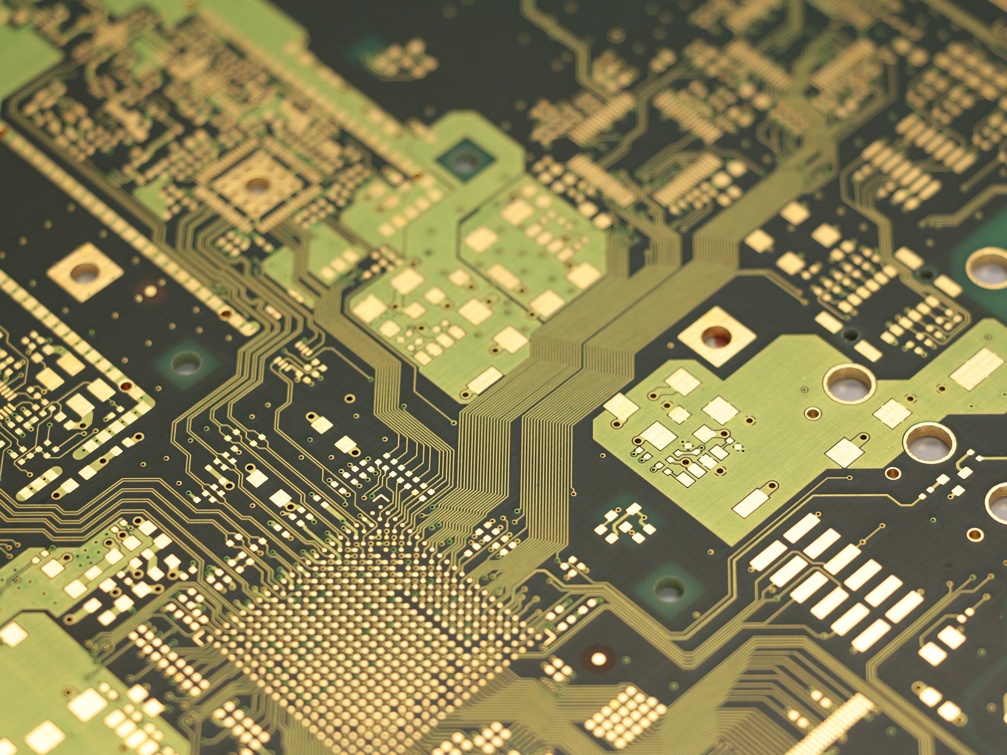

LIMATA laser direct system (LDI) solutions can be used during the maskless direct imaging process for all standard and advanced PCB applications (dry-film patterning) including:
- Advanced PCBs (HDI) and IC substrates designs
- Finest feature sizes and gaps down to 12μm / 0.5 mil with industrial imaging speed
Standard PCB designs (MLB, FPCB)
- Finest feature sizes and gaps down to 12μm / 0.5 mil with industrial imaging speed
- Standard PCB designs (MLB, FPCB)
- Multi Layer Boards down to 25 um L/S / 1.0 mil in PCB production
at high-throughput
- Multi Layer Boards down to 25 um L/S / 1.0 mil in PCB production
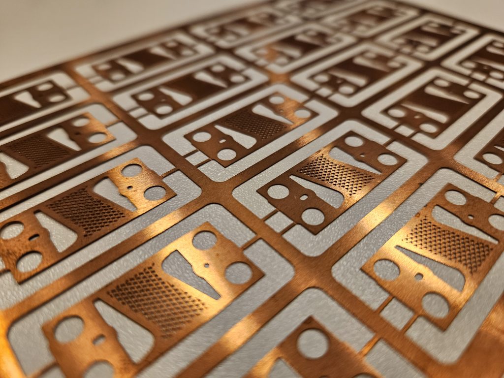
- Chem-Mill / High-Precision etched parts
- Highly-accurate front to back alignment (10μm / 0.4mil)