Limata

Products
Applications
Services
Company

About us

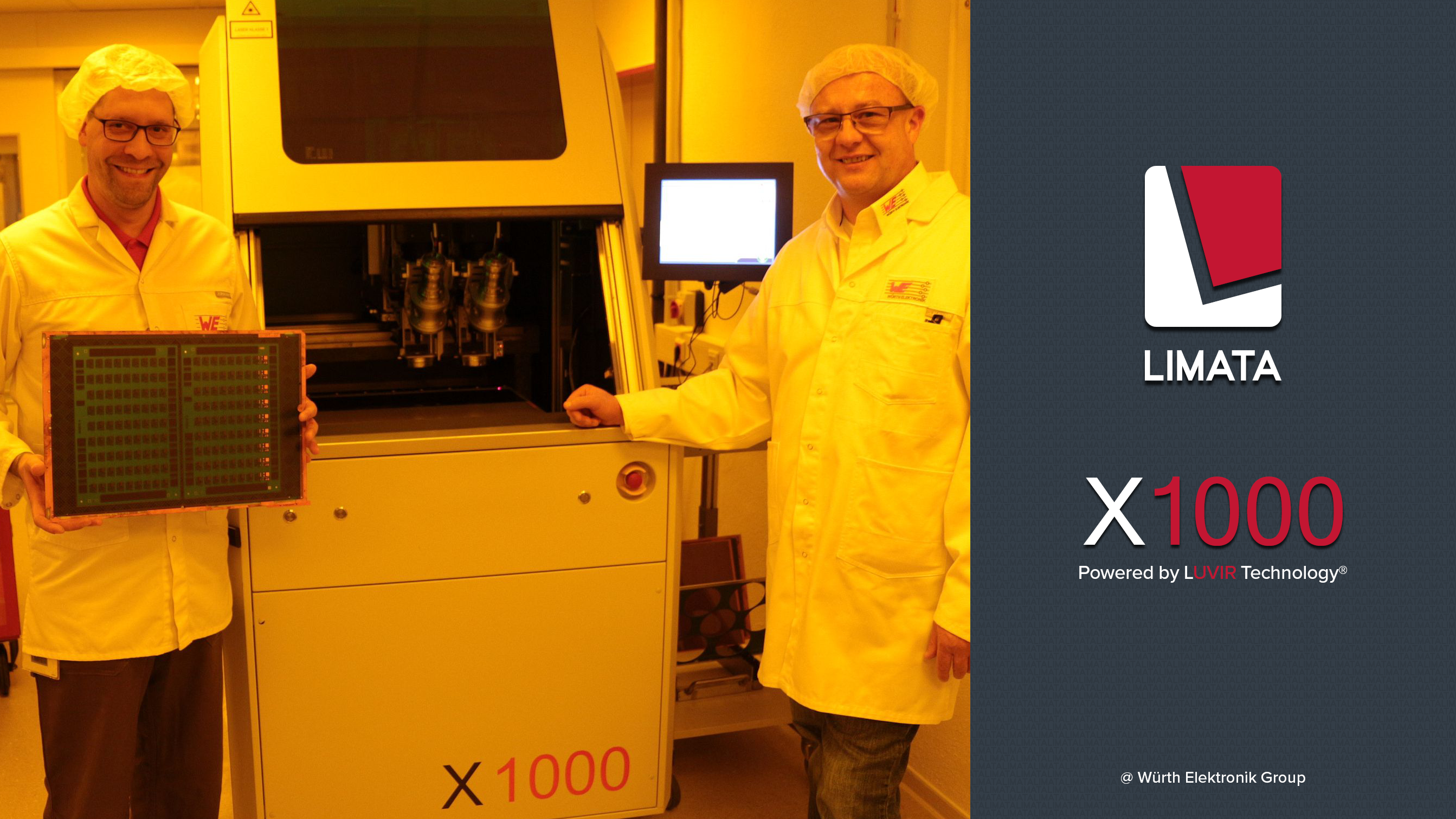
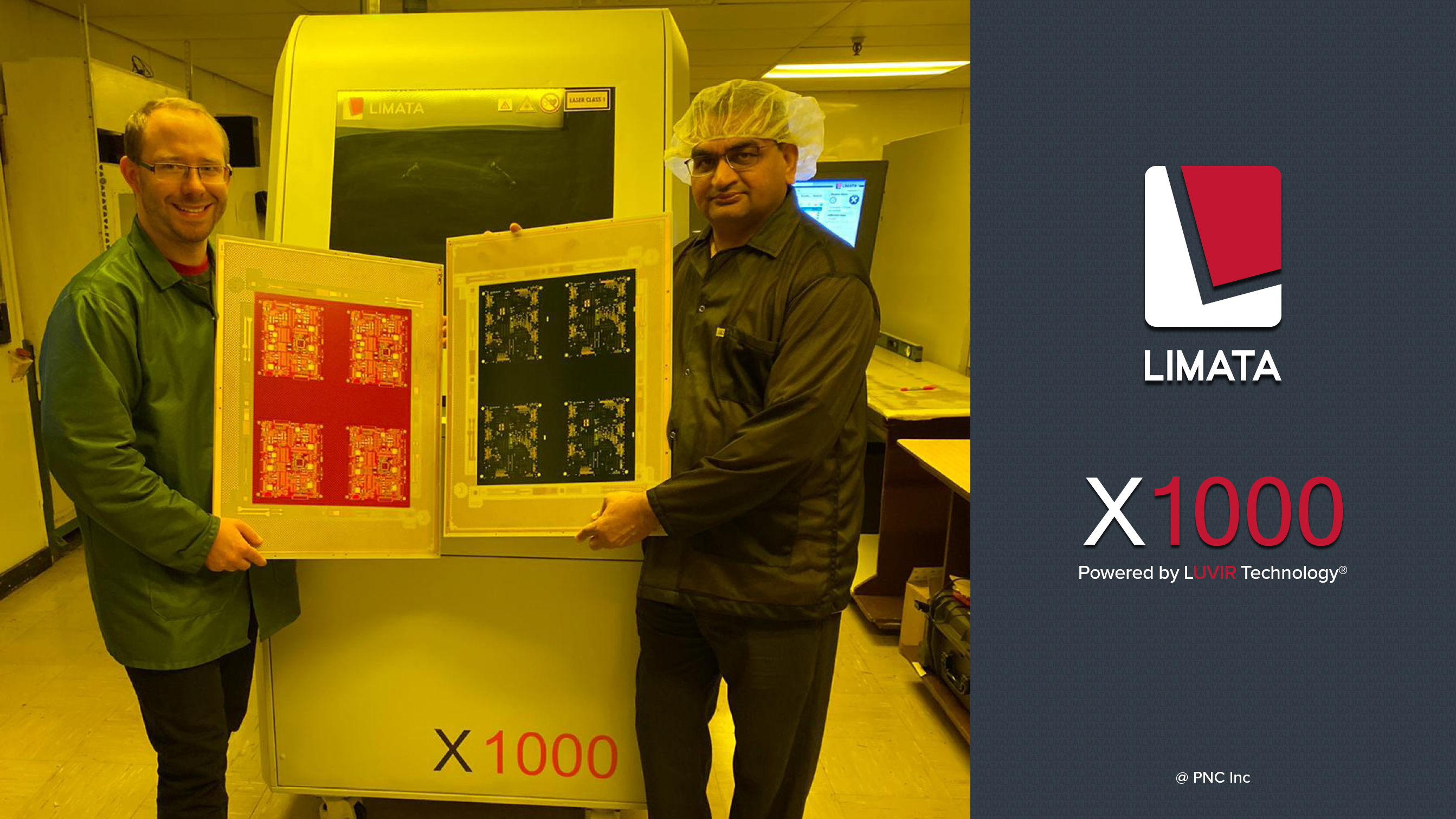
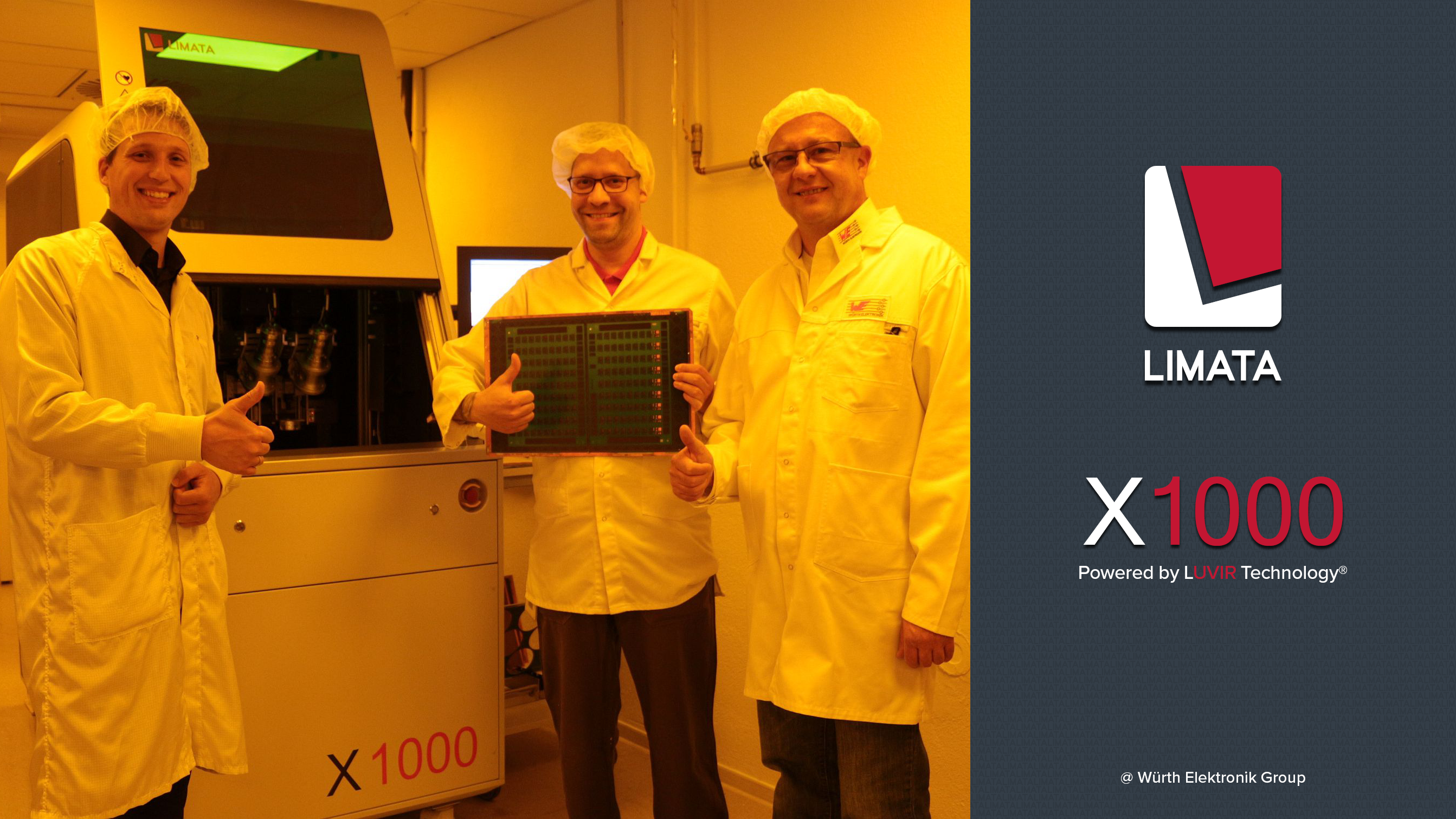
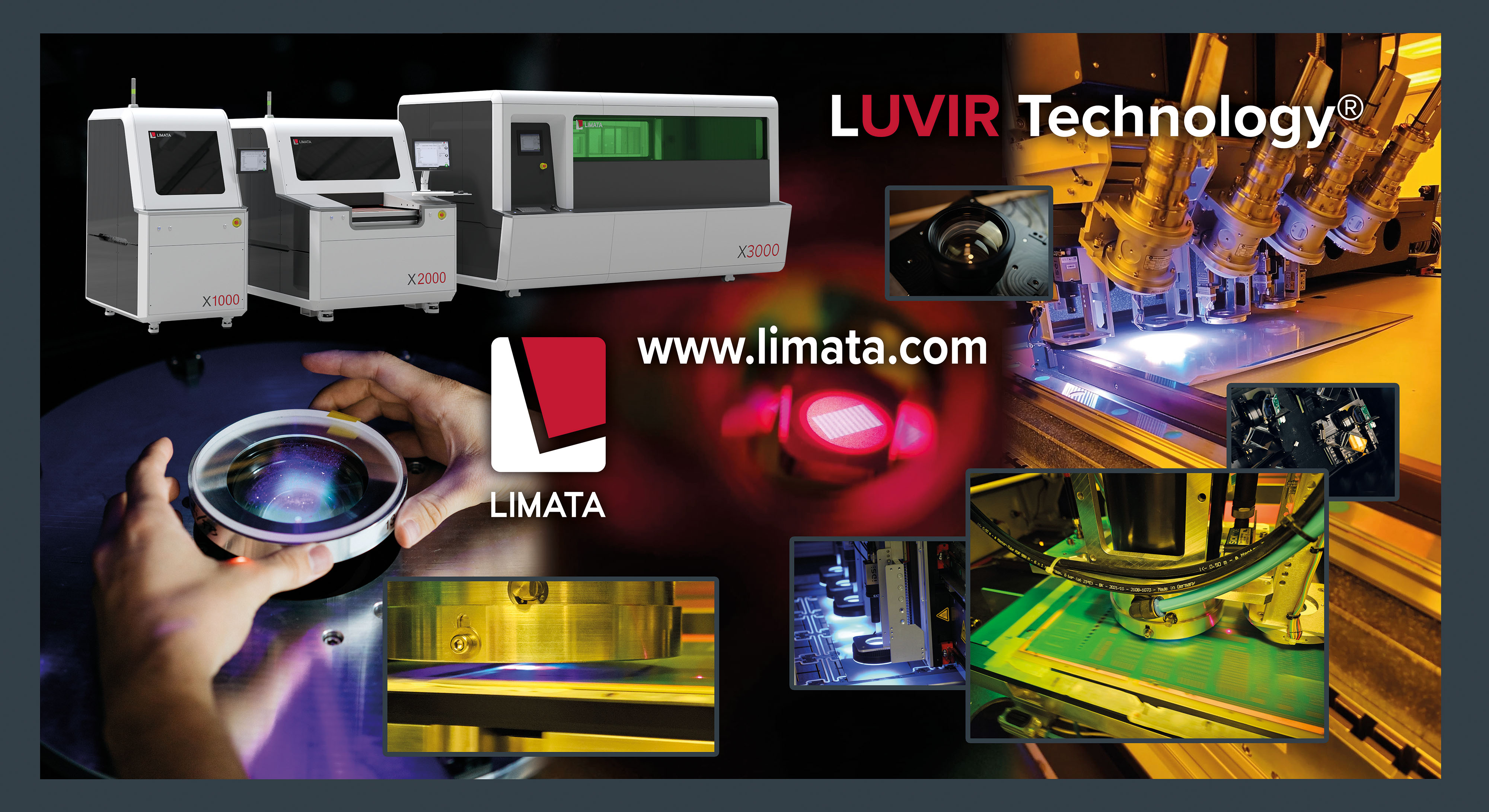
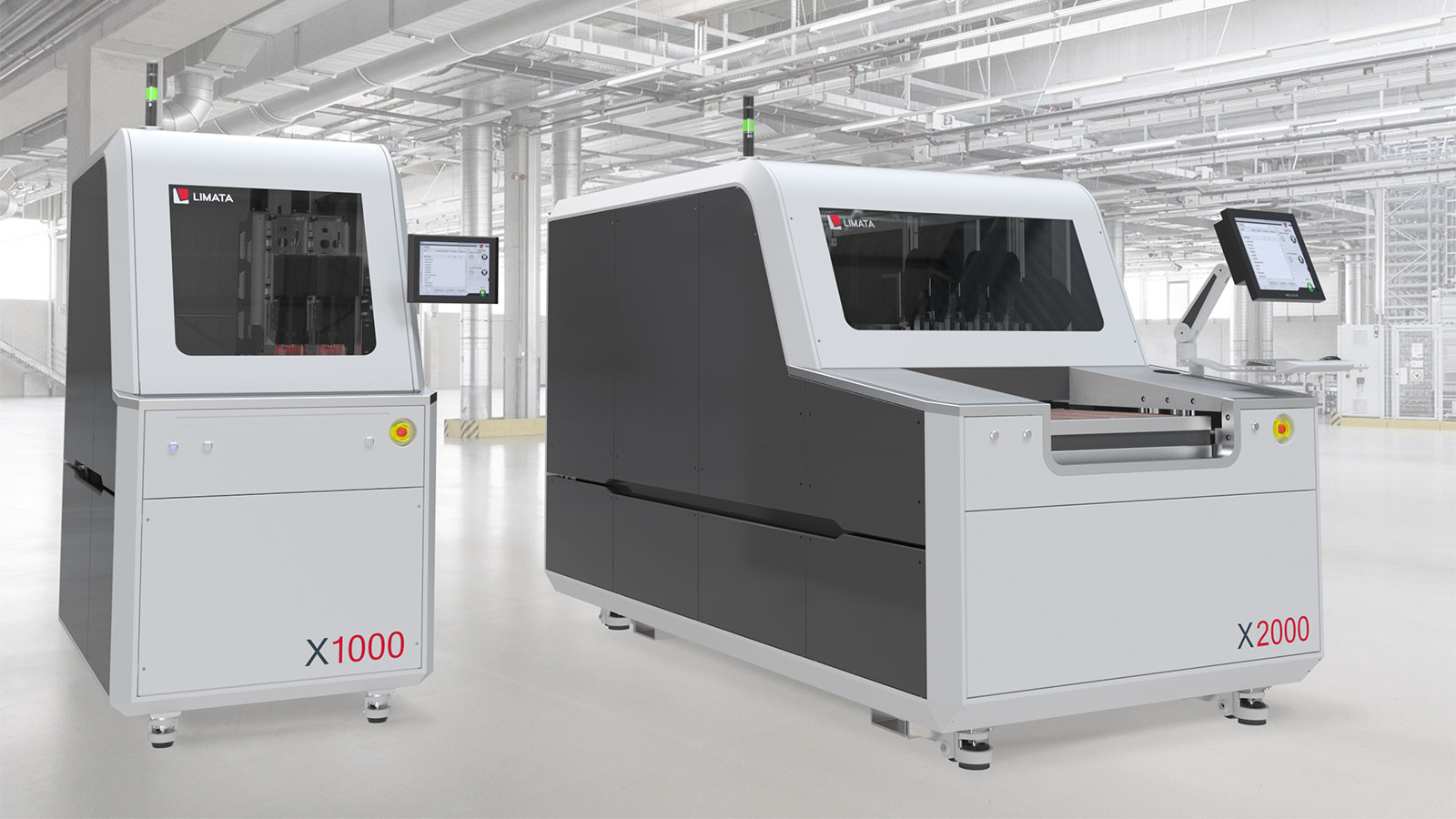
We are an innovative supplier of laser direct imaging (LDI) system solutions for various PCB manufacturing environments and adjacent markets. Our system product portfolio ranges from LDI system configurations for high-mix and emerging PCB niche applications up to fully automated LDI system solutions for mass production environments.

We are an entrepreneurial, innovation and customer driven organization with staff, operations and/or value adding sales partnerships in all key PCB manufacturing regions. The core of our operation is Ismaning near Munich (Germany) which is also home to our R&D/development, engineering and applications team.

Your solutions provider for direct imaging

Based on our in-house developed direct imaging technology combined with an advanced and modular configureable hardware system platform (X-Series), LIMATA direct imaging solutions enable PCB manufacturers to maintain high production yields and to increase image quality and output for standard and advanced PCB applications at lower cost of ownership over the DI equipment lifecycle. We are committed to closely working and partner with our customers and stretch ourselves in order to deliver the best DI solution for their PCB application and process (or to solve their problem).

Delivering smart system solutions for your PCB imaging process

Your individual PCB product application and process requirements are key.

The customization of our DI system products with innovative imaging concepts, optimized hardware and automation features, IoT data processing interfaces and technological advancements are one of our core expertises. This approach allows us to align to your individual imaging needs and to continously adapt to new market requirements („time-to-market“).

Selected customer references

Click on Image to read Statements

WÜRTH ELEKTRONIK GROUP

WÜRTH ELEKTRONIK GROUP (Circuit Board Technology) chooses a LIMATA X1000 system solution (powered by LUVIR®) to fully digitalize the solder mask process at its Rot am See site.

Ralf Göhringer (Head of Production WE Rot am See) stated:
„Thanks to the LUVIR technology, the solder resist process could be switched directly from the previously used mask exposure to direct exposure. As an outstanding digital solution on the market, this technology has been able to demonstrate fast process times and superior quality on our certified conventional ink in production. This allowed us to fully digitize the solder mask process at low cost – without process or ink adjustments. An excellent benefit to our production in Rot am See.“

PNC Inc.

LIMATA X1000 Powered by LUVIr Technology at PNC Inc

PNC INC chooses a LIMATA X1000 system solution (powered by LUVIR®) for their Solder Mask/Silk Screen process at its US Nutley, NJ site.

Sam Sangani (President of PNC) stated:
“LIMATA´s X1000 system solution powered by LUVIR technology® fully convinced our engineering team during the evaluation and production phase. We evaluated all available solutions for the Solder Mask and Silk Screen processes, and we determined that LIMATA is by far, the most economical and the fastest machine with unmatched imaging quality in our industry. The capacity, flexibility and cost/performance ratio of the X1000 LUVIR DI system is outstanding in the market and offers PNC the ability to produce PCBs fully digital at significantly higher throughput levels by meeting all state-of-the art quality requirements for Solder Mask/ Silk Screen imaging”.

LIMATA Direct Imaging Solutions

Increased technical requirements in PCB manufacturing driven by more advanced PCB designs (towards thinner materials, more complex and finer structures at only small design rule tolerances) have set limitations for the conventional mask contact lithography (phototool) method in particular for the production of more advanced PCB applications.

This has led to a shift in production technology from conventional mask contact lithography to the Maskless Direct Imaging of PCBs, where a software controlled laser or light-source is used to image a pattern directly on a photoresist coated panel or to image liquid solder mask/resist layers at the backend of the PCB manufacturing process.

Key advantages of the Direct Imaging (DI) technology include:

  • Higher accuracy in registration as well as printing (line uniformity)
  • Higher depth-of-focus
  • Full product and process traceability during the manufacturing process (data interfaces)
  • Higher productivity and quality levels (throughput and yields) during PCB production
  • Lower process costs and total costs of ownership versus conventional mask/film lithography during the pattern or solder mask process

Backed by a dedicated in-house hardware & software engineering team, LIMATA has developed a complete DI system product line for the PCB patterning and solder mask process. In addition and after a joint application/process analysis, LIMATA provides its international PCB customer base with system customizations, MES-interface programming services and complementary automation solutions.

Key imaging components used in LIMATA‘s system solutions consisting of DMD/DLP units, UV-LED & Laser diodes and optics have been either developed internally or in-close cooperation with key component suppliers. A fully in-house developed software platform completes LIMATA‘s system product offerings.